powerpcb使用簡介

1.用Add
Ans:此 marker通常是提醒你在 component rule作過設(shè)定,記得作design Verification check 若無設(shè)定而 verify design check 出現(xiàn)此marker應(yīng)是v5.0 版本的bug
4. 若零件pad是由pad與copper作associate則自動鋪銅時pad無法形成thermal
Ans:不會形成thermal
5. 若零件pad是由pad與copper作associate,在出底片作cam 時應(yīng)在solder mask選擇Top 'pin withassociate copper'advanced selsction'pads 'filled copper
此時 solder mask 會出現(xiàn)pad+copper 的形狀
(不受copper 與pad associate需包含整個pad 的限制)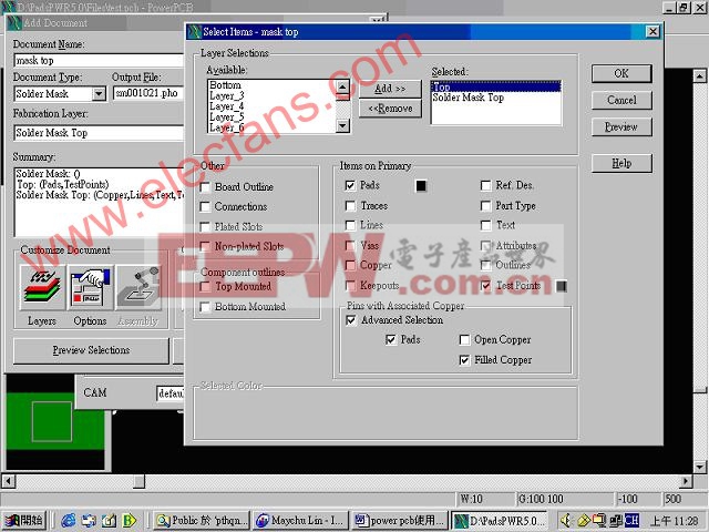
6. pcb 的設(shè)計若為HDI ,via需打在pad上,則可按下mouse右key彈出 menu ,select add via 或按shift_click 使via打在pad 上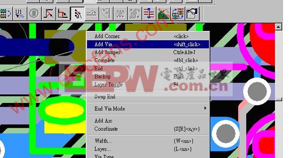

評論